MOS 6522 Versatile Interface Adapter


OCR Source: Archive.org mos_6560_6561_vic.pdf. Some spelling mistakes may remain due to the poor quality of the source material.
MCS6522 VERSATILE INTERFACE ADAPTER
DESCRIPTION
The MCS6522 Versatile Interface Adapter (VIA) provides all of the capability of the MCS6520. In addition, this device contains a pair of very powerful interval timers, a serial-to-parallel/ parallel-to-serial shift register and input data latching on the peripheral ports. Expanded handshaking capability allows control of bi-directional data transfers between VIA's in multiple processor systems.
Control of peripheral devices is handled primarily through two 8-bit bi-directional ports. Each of these lines can be programmed to act as either an input or an output. Also, several peripheral I/O lines can be controlled directly from the interval timers for generating programmable-frequency square waves and for counting externally generated pulses. To facilitate control of the many powerful features of this chip, the internal registers have been organized into an interrupt flag register, an interrupt enable register and a pair of function control registers.
- Very powerful expansion of basic MCS6520 capability.
- N channel, depletion load technology, single +5V supply.
- Completely static and TTL compatible.
- CMOS compatible peripheral control lines.
- Expanded "handshake" capability allows very positive control of data transfers between processor and peripheral devices.
PROCESSOR INTERFACE
This section contains a description of the buses and control lines which are used to interface the MCS6522 to the system processor. AC and DC parameters associated with this interface are specified on pages 21 through 24 of this document.
PHASE TWO CLOCK (02)
Data transfers between the MCS6522 and the system processor take place only while the Phase Two Clock is high. In addition, 02 acts as the time base for the various timers, shift registers, etc. on the chip.
CHIP SELECT LINES (CS1, CS2)
The two chip select inputs are normally connected to processor address lines either directly or through decoding. The selected MCS6522 register will be accessed when CS1 is high and CS2 is low.
REGISTER SELECT LINES (RSO, RSI, RS2, RS3)
The four Register select lines are normally connected to the processor address bus lines to allow the processor to select the internal MCS6522 register which is to be accessed. The sixteen possible combinations access the registers as follows:
| Address | RS3 | RS2 | RS1 | RS0 | Register | Remarks |
|---|---|---|---|---|---|---|
| 0 | 0 | 0 | 0 | 0 | ORB | |
| 1 | 0 | 0 | 0 | 1 | ORA | |
| 2 | 0 | 0 | 1 | 0 | DDRB | |
| 3 | 0 | 0 | 1 | 1 | DDRA | |
| 4 | 0 | 1 | 0 | 0 | ||
| 5 | 0 | 1 | 0 | 1 | ||
| 6 | 0 | 1 | 1 | 0 | ||
| 7 | 0 | 1 | 1 | 1 | ||
| 8 | 1 | 0 | 0 | 0 | ||
| 9 | 1 | 0 | 0 | 1 | ||
| A | 1 | 0 | 1 | 0 | ||
| B | 1 | 0 | 1 | 1 | ||
| C | 1 | 1 | 0 | 0 | ||
| D | 1 | 1 | 0 | 1 | ||
| E | 1 | 1 | 1 | 0 | ||
| F | 1 | 1 | 1 | 1 |
READ/WRITE LINE (R/W)
The direction of data transfers between the MCS6522 and the system processor is controlled by the R/W line. If R/W is low, data will be transferred out of the processor into the selected MCS6522 register (write operation). If R/W is high and the chip is selected, data will be transferred out of the MCS6522 (read operation).
DATA BUS (D0 - D7)
The 8 bi-directional data bus lines are used to transfer data between the MCS6522 and the system processor. The internal drivers will remain in the high-impedance state except when the chip is selected (CS1 = 1, CS2 = 0), R/W is high and the Phase Two Clock is high. At this time, the contents of the selected register are placed on the data bus. When the chip is selected, with R/W low and ∅2 = 1, the data on the data bus will be transferred into the selected MCS6522 register.
RESET (RES)
The Reset input clears all internal registers to logic 0 (except Tl, T2 and SR). This places all peripheral interface lines in the input state, disables the timers, shift register, etc. and disables interrupting from the chip.
INTERRUPT REQUEST (IRQ)
The Interrupt Request output goes low whenever an internal interrupt flag is set and the corresponding interrupt enable bit is a logic 1. This output is "open-drain" to allow the interrupt request signal to be "wire-or'ed" with other equivalent signals in the system.
PERIPHERAL INTERFACE
This section contains a brief description of the buses and control lines which are used to drive peripheral devices under control of the internal MCS6522 registers.
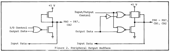
PERIPHERAL A PORT (PA0 - PA7)
The Peripheral A port consists of 8 lines which can be individually programmed to act as an input or an output under control of a Data Direction Register. The polarity of output pins is controlled by an Output Register and input data can be latched into an internal register under control of the CA1 line. All of these modes of operation are controlled by the system processor through the internal control registers. These lines represent one standard TTL load in the input mode and will drive one standard TTL load in the output mode.
PERIPHERAL A CONTROL LINES (CA1, CA2)
The two peripheral A control lines act as interrupt inputs or as handshake outputs. Each line controls an internal interrupt flag with a corresponding interrupt enable bit. In addition, CA1 controls the latching of data on Peripheral A Port input lines. The various modes of operation are controlled by the system processor through the internal control registers. CA1 is a high-impedance input only while CA2 represents one standard TTL load in the input mode. CA2 will drive one standard TTL load in the output mode.
PERIPHERAL B PORT (PB0 - PB7)
The Peripheral B port consists of 8 bi-directional lines which are controlled by an output register and a data direction register in much the same manner as the PA port. In addition, the polarity of the PB7 output signal can be controlled by one of the interval timers while the second timer can be programmed to count pulses on the PB6 pin. These lines represent one standard TTL load in the input mode and will drive one standard TTL load in the output mode. In addition, they are capable of sourcing 30 ma at 1.5 VDC in the output mode to allow the outputs to directly drive Darlington transistor switches.
PERIPHERAL B CONTROL LINES (CB1, CB2)
The Peripheral B control lines act as interrupt inputs or as handshake outputs. As with CA1 and CA2, each line controls an interrupt flag with a corresponding interrupt enable bit. In addition, these lines act as a serial port under control of the Shift Register. These lines represent one standard TTL load in the input mode and will drive one standard TTL load in the output mode. In addition, they are capable of sourcing 1.0 ma at 1.5 VDC in the output mode to allow the outputs to directly drive Darlington transistor switches.
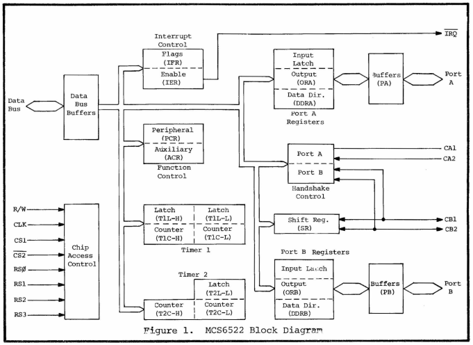
MCS6522 OPERATION
This section contains a discussion of the various blocks of logic shown in Figure 1. In addition, the internal operation of the MCS6522 is described in detail.
DATA BUS BUFFERS (DB), PERIPHERAL A BUFFERS (PA), PERIPHERAL B BUFFERS (PB)
The characteristics of the buffers which provide the required voltage and current drive capability were discussed in the previous section. -AC and DC parameters for these buffers are specified on pages 21 through 24 of this document.
CHIP ACCESS CONTROL
The Chip Access Control contains the necessary logic to detect the chip select condition and to decode the Register Select inputs to allow accessing the desired internal register. In addition, the R/W and ∅2 signals are utilized to control the direction and timing of data transfers. When writing into the MCS6522, data is first latched into a date, input register during ∅2. Data is then transferred into the desired internal register during ∅2 CS. This allows the peripheral I/O line to change without "glitching." When the processor reads the MCS6522, data is transferred from the desired internal register directly onto the Data Bus during ∅2.
PORT A REGISTERS, PORT B REGISTERS
Three registers are used in accessing each of the 8-bit peripheral, ports. Each port has a Data Direction Register (DDRA, DDRB) for specifying whether the peripheral pins are to act as inputs or outputs. A 0 in a bit of the Data Direction Register causes the corresponding peripheral pin to act as an input. A 1 causes the pin to act as an output.
Each peripheral pin is also controlled by a bit in the Output Register (ORA, ORB) and an Input Register (IRA, IRB). When the pin is programmed to act as an output, the voltage on the pin is controlled by the corresponding bit of the Output Register. A 1 in the Output Register causes the pin to go high, and a 0 causes the pin to go low. Data can be written into Output Register bits corresponding to pins which are programmed to act as inputs; however, the pin will be unaffected.
Reading a peripheral port causes the contents of the Input Register (IRA, IRB) to be transferred onto the Data Bus. With input latching disabled, IRA will always reflect the data on the PA pins. With input latching enabled, IRA will reflect the contents of the Port A prior to setting the CA1 Interrupt Flag (IFRl) by an active transition on CA1.
The IRB register operates in a similar manner. However, for output pins, the corresponding IRB bit will reflect the contents of the Output Register bit instead of the actual pin. This allows proper data to be read into the processor if the output pin is not allowed to go to full voltage. With input latching enabled on Port B, setting CB1 interrupt flag will cause IRB to latch this combination of input data and ORB data until the interrupt flag is cleared.
HANDSHAKE CONTROL
The MCS6522 allows very positive control of data transfers between the system processor and peripheral devices through the operation of "handshake" lines. Port A lines (CA1, CA2) handshake data on both a read and a write operation while the Port B lines (CB1, CB2) handshake on a write operation only.
Read Handshake
Positive control of data transfers from peripheral devices into the system processor can be accomplished very effectively using "Read" handshaking. In this case, the peripheral device must generate "Data Ready" to signal the processor that valid data is present on the peripheral port. This signal normally interrupts the processor, which then reads the data, causing generation of a "Data Taken" signal. The peripheral device responds by making new data available. This process continues until the data transfer is complete.
In the MCS6522, automatic "Read" handshaking is possible on the Peripheral A port only. The CAl interrupt input pin accepts the "Data Ready" signal and CA2 generates the "Data Taken" signal. The Data Ready signal will set an internal flag which may interrupt the processor or which can be polled under software control. The Data Taken signal can be either a pulse or a DC level which is set low by the system processor and is cleared by the Data Ready signal. These options are shown in Figure 3 which illustrates the normal Read Handshaking sequence.
Write Handshake
The sequence of operations which allows handshaking data from the system processor to a peripheral device is very similar to that described in Section A for Read Handshaking. However, for "Write" handshaking, the processor must generate the "Data Ready" signal (through the MCS6522) and the peripheral device must respond with the "Data Taken" signal. This can be accomplished on both the PA port and the PB port on the MCS6522. CA2 or CB2 acts as a Data Ready output in either the DC level or pulse mode and CA1 or CB1 accepts the "Data Taken" signal from the peripheral device, setting the interrupt flag and clearing the "Data Ready" output. This sequence is shown in Figure 4.